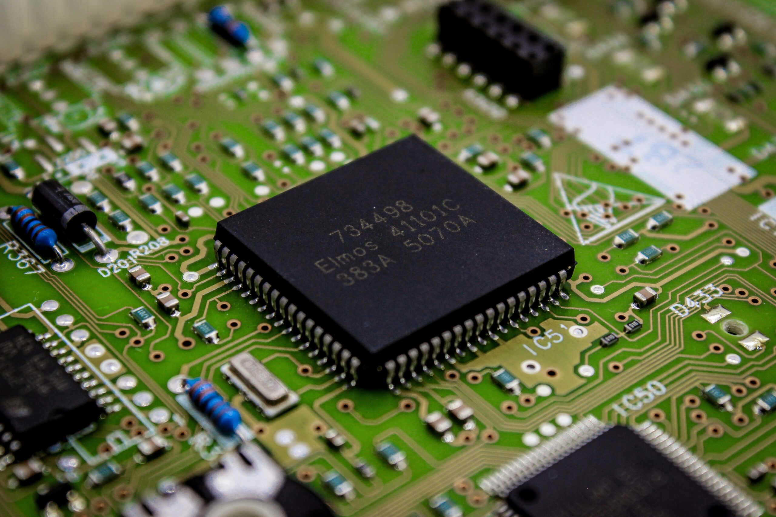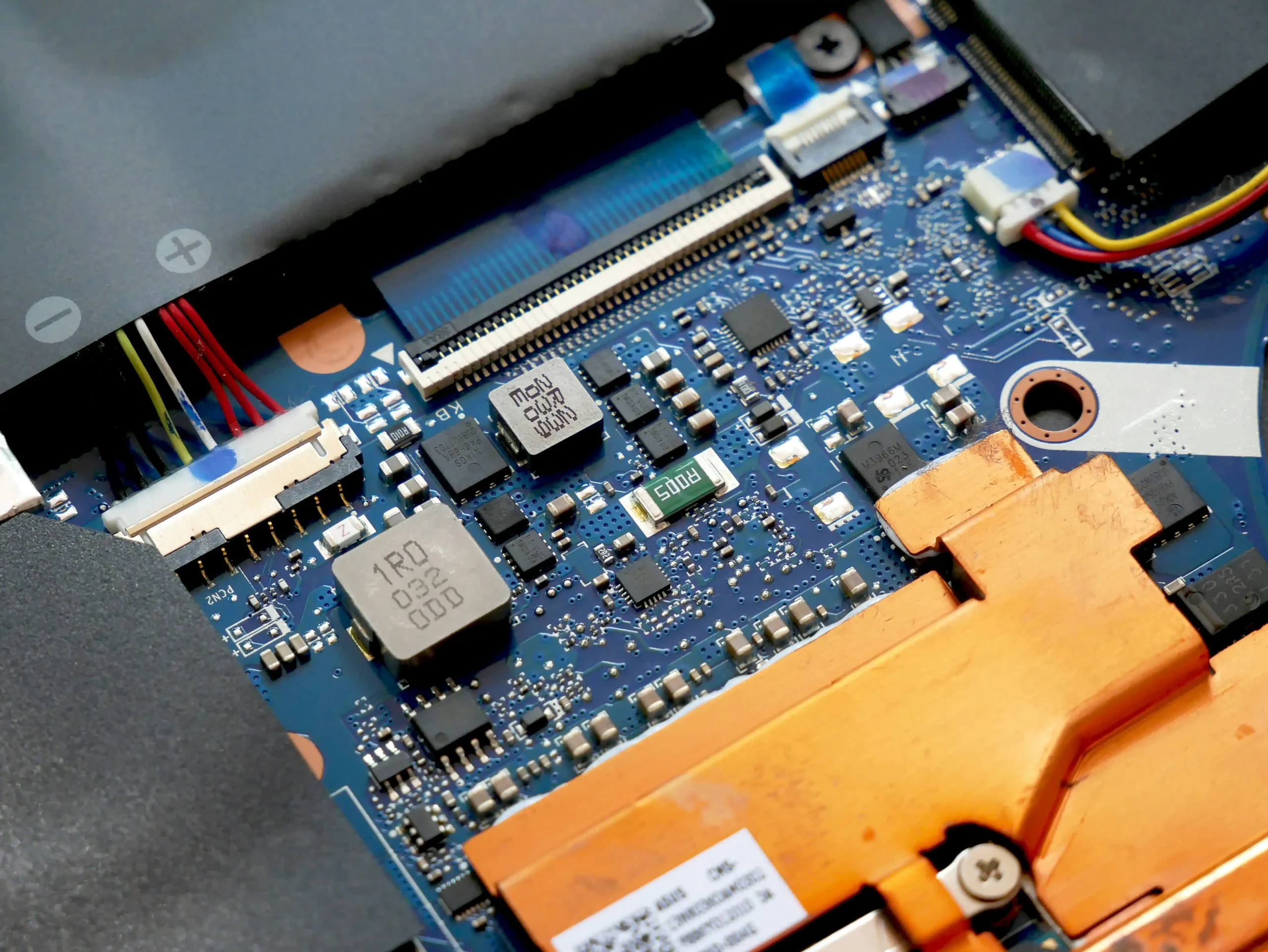
GaN semiconductor manufacturing in India is advancing rapidly, with one of Zephyr Peacock India’s portfolio companies Agnit Semiconductors emerging as a pioneering player in the country’s semiconductor ecosystem. In our view, the company develops Gallium Nitride (GaN) chips, a next-generation technology with clear performance advantages over traditional silicon. GaN enables significantly higher electron mobility, higher voltage tolerance, and better thermal conduction, making it useful for high-power, high-frequency applications in radio frequency (RF) and power electronics. (1)
Agnit has access to one of only two GaN fabrication foundries in India, located at the Indian Institute of Science (IISc), a premier university in India. The company designs and manufactures its own wafers, processing them through dicing, assembly, packaging, and testing. Unlike conventional semiconductors, GaN wafers are challenging to produce and often require specialized substrates (1), which form the base materials on which chips are built an essential capability for strengthening GaN semiconductor manufacturing in India.
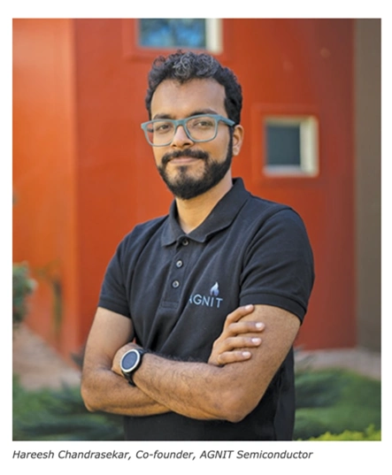
Agnit aims to make locally manufactured GaN devices viable for both RF communications and power conversion systems, such as efficient fast chargers. The company is also exploring opportunities beyond defense and telecom, experimenting with compact and efficient GaN-based EV charging solutions that potentially could outperform silicon-based equivalents. “We are still testing; the potential is massive. If this scales, the next EV charger could fit in a backpack—smaller, faster, and far more efficient than anything silicon can do today,” commented Hareesh Chandrasekar, CEO and Founder of Agnit Semiconductors.
GaN Semiconductor Manufacturing in India and the Shift to Device Fabrication
Agnit exemplifies India’s transition from design-only semiconductor services to full-scale materials and device fabrication. In a fast-growing global GaN market, the company’s progress in GaN semiconductor manufacturing in India, from lab-scale innovation to fabrication-ready devices, positions it to participate meaningfully in the highest-value layers of the semiconductor ecosystem in our view.
At Zephyr Peacock India, we believe innovation-led transformation driven by productivity, technology, and value creation will define the next wave of investment opportunities for advanced manufacturing PE firms in India.
Read more in this article, which first appeared on Electronics For U
A semiconductor wafer is a thin slice of semiconductor substance used in electronics for producing integrated circuits.
(1) Source: Electronics For U
“This content is Intended for Informational purposes only and does not constitute an offer to sell or invitation to purchase any securities or interests in any investment funds managed by Zephyr. The information provided herein is shared with the understanding that It is not meant to serve as a public invitation or endorsement to engage in any specific investment activity.”